Research
Coming from a physics background my research interests are spread across different fields covering physics, chemistry material science and nanotechnology.
A major focus of interest are structure-function relations of organic and hybrid (organic-inorganic) materials that are used for energy applications, mainly solar cells and also further related applications such as sensors and energy storage applications which can tremendously benefit from functional nanostructured materials. Our research involves several aspects from photophysics, material processing and its characterisation to its final application in devices, covering fundamental questions to engineering challenges.
Research Topics
- Organic Photovoltaics
- Hybrid Photovoltaics
- Material Processing
- Structure-Function Relations of Nanostructured Materials
- Optoelectronics
- Transistors and Sensors
- Organic PhotovoltaicsHide
-
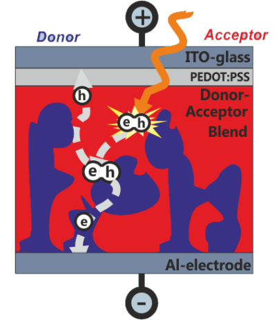
Organic solar cells are based on conjugated molecules, polymers or fullerenes that act as a donor or an acceptor material. Organic solar cells are very promising due to their ease of processability for example via printing, their compatibility with flexible substrates and their low environmental impact during procesing (very short energy payback time). Excitons can be separated at the interface between the acceptor and donor material and charges are created. An efficient charge separation required organic semiconductors with the right energy levels as well as a nanomorphology accounting for the short exciton diffusion length (~10 nm).
We investigate novel semiconducing polymers, characerize theri electrical and strucutral properties and look at the donor-acceptor interplay to build efficient organic solar cells.
- Hybrid PhotovoltaicsHide
-
Hybrid metal halide perovskites have become one of the hottest topics in optoelectronic materials research in recent years. Not only have they surpassed everyone’s expectations and achieved similar performance as tried and true polycrystalline silicon photovoltaic devices, but they are also finding applications in a wide variety of different fields including light emitting diodes (LEDs). The main advantages of hybrid metal halide perovskites are its simple processability, compatible with large-scale solution processing such as roll-to-roll printing, abundance of its ingredients. Solar efficiencies of more than 22% have been reparted recently.
- Material ProcessingHide
-
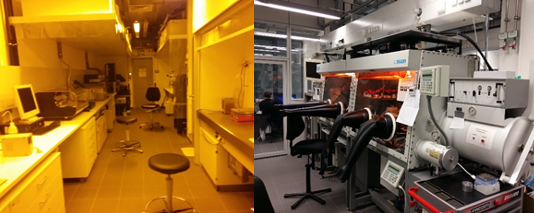
The Keylab "Device Engineering" offers the latest state of the art materials processing equipment to fabricate thin films, evaporate electrodes and pattern electronic devices.
We are using self-assembling processes in polymer systems such as micro phase separation or phase separation through crystallisation is used to pattern functional nanostructures. For perovskites we control the crystallisation kinetics to achieve differnt crystal sizes from nm range to macroscopic single crystals in the mm range.